Insulator Defects Observable by Scanning Tunneling Microscopy
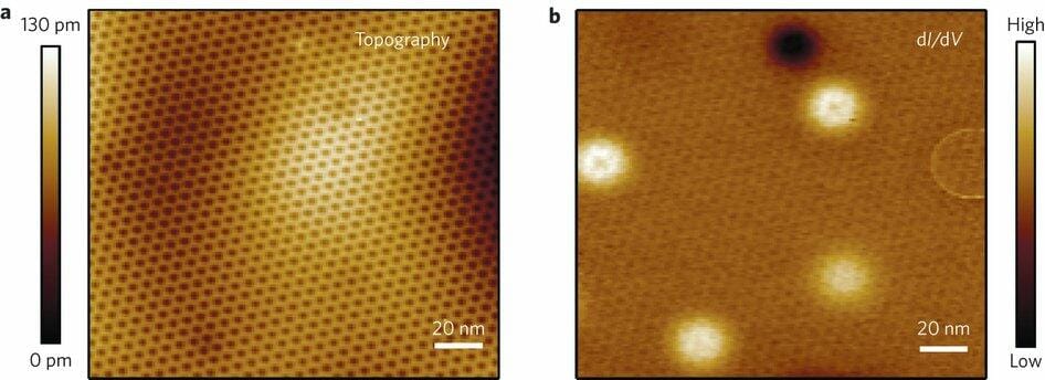
(a) STM image of graphene/BN (b) dI/dV map obtained together with (a) has new dots and rings.
Researchers from the Lawrence Berkeley National Laboratory and the University of California at Berkeley have characterized individual defects in an insulator using scanning tunneling microscopy (STM). The researchers covered the bulk insulator with a graphene layer that transmitted the current -necessary for STM observation- to the insulator surface. The findings have been published in the journal Nature Nanotechnology.
Nanoscale materials must be thoroughly tested for individual defects that could affect its properties and applications. Defects are usually very localized, and ideally they should be characterized at single-level. Conductors and semi-conductors are usually checked for defects with STM, a technique that images the material surface at atomic level. In STM, a conducting tip is placed at a very short distance from the surface to be analyzed, and a voltage difference is applied to cause electrons to travel in the vacuum between the surface and the tip. The tunneling current informs about the structure as the tip scans the surface. With a 0.01 nm depth resolution, individual atoms can be imaged and manipulated, and the electronic structure of point defects can be detected. The problem arises when trying to characterize bulk insulators, which by definition do not allow electrical current to flow through them.
An ultra-thin graphene sheet over the h-BN insulator to visualize its defects
Hexagonal boron nitride (h-BN) is a crystalline compound extensively used as an insulator, with excellent thermal and chemical stability. Due to its properties, it is not a suitable material for STM observation; instead of defining individual point defects, defect behaviors must be spatially averaged. This technique could soon be obsolete thanks to Dr. Crommie and colleagues. To make h-BN visible to STM, Dr. Crommie’s team covered the insulator surface with a graphene/boron nitride layer. The conductive properties of graphene, together with the ultra-thin nature of the layer, allowed the current to reach the H-BN surface underneath and to observe its individual defects. This is possible because STM detects how electrons in graphene react to defects in h-BN. With this technique, the research team was able to observe three different defect structures that can be ascribed to defects in the h-BN insulator. They were also able to modify the defects by sending voltage pulses through the STM tip.
The new technique will be extremely useful for nanoengineering laboratories that use h-BN or other insulators.
Source: Berkeley Lab