New Super-Thin Nanocrystalline Membrane to Advance Lab-on-Chip Technology


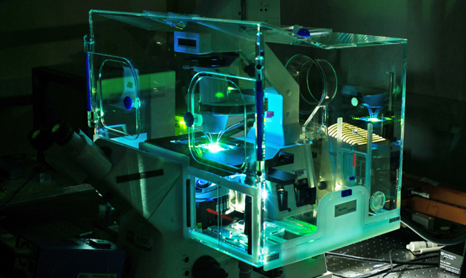
This device is a flow-based cell co-culturing system consisting of two chambers separated by a nanoporous silicon membrane. It allows to perform in situ cell manipulation, optical imaging, flow-based assays using minimal amounts of reagent and the ultrathin silicon membrane provides an excellent mimic of the biological barrier properties. (Photo by J. Adam Fenster / University of Rochester)
By using porous nanocrystalline silicon (pnc-Si) membranes, researchers from the University of Rochester have found a way to shrink laboratory scale processes to run on small chip like systems. Advancements in the lab-on-chip technology have a direct bearing on advancements in biotechnology and medicines.
In lab-on-chip devices, electroosmotic pumps (EOPs) are responsible for the movement of solutions through microchannels. In EOPs, electroosmotic flow makes the fluids flow through channels placed in between the electrodes. The interaction between electric field and ions on a charged surface is responsible for this flow. The conventional porous membranes used between these electrodes cause significant voltage drops between them, forcing the use of larger high voltage power sources to overcome the voltage drop, affecting the device size.
The pnc-Si membranes are so thin that one has to stack at least a thousand of them, one up on another to attain the width of a human hair. These microscopically thin membranes are ideal for developing low-voltage systems. Thus, by using these pnc-Si membranes between the electrodes, EOPs can be operated at voltages as low as 0.25 V as against the 10 kV requirements for those with conventional membranes, thereby drastically reducing the size of power source required to run them. This in turn affects the overall size of the devices. With the pnc-Si membrane, and smaller, more efficient EOPs, it is now possible to develop a wide range of inexpensive credit card sized lab-on-chip diagnostic devices.
Source: University of Rochester
