3D Nanosculptures Created with Electron Microscopy

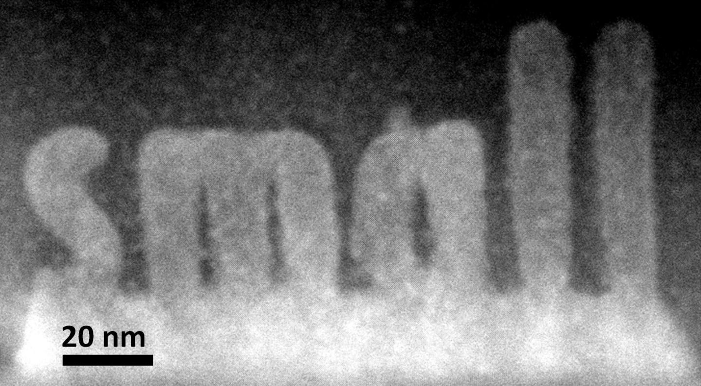
STEM-designed 3D nanosculpture in complex oxide material. Credit: ORNL
Researchers from Oak Ridge National Laboratory (ORNL) have developed a method to design 3D sculptures at atomic level with an electron microscope. The crystalline structures size is between 1 and 2 nm and the creation process can be followed in real time with atomic resolution. The structure can be shaped at will modifying the electron beam speed and position. The study was published in the journal Small.
Electron microscopes are imaging tools that use electrons instead of photons as a source of illumination. Thanks to the electron´s smaller wavelength, electron microscopes have a higher resolving power and can show smaller structures. ORNL researchers were working with a strontium titanate film made of a crystalline structure covered with an amorphous layer. When they directed the electron beam to the surface, they unexpectedly found that it acquired a crystalline arrangement.
The electron beam transfers energy and accelerates thermodynamic processes
The Titan supercomputer simulations helped the researchers understand the molecular mechanism of the phenomenon observed in this study. In STEM, the electron beam transfers an amount of energy to the atoms that accelerates the thermodynamic preference of the system. The amorphous layer would eventually adopt the crystalline structure, but it would take it much more time.
Common litography techniques can manipulate the structure of a material´s surface. By contrast, in scanning transmission electron microscope (STEM) electrons can go through the material and manipulate its interior. This characteristic will also allow to observe how materials properties change depending on their thickness, without the need of adding layers between measurements.
The new technique can be used to sculpt nanostructures in oxide materials. The designs grow orderly in crystalline alignment, so the whole structure has the same electrical and mechanical properties. The method allows to create smaller things with higher precision than with current nanosculpting techniques, and it could be used to build functional nanostructures like microchips.
Source: ORNL